Xbox One PadHack Thread - Calling the goons "Toodles, Gummowned, Phreak and You" Do it for the Kids

No, he’s talking about Y1, the square gold thing to the left of where you are pointing that has 4 pads.

If you kill the oscillator the micro won’t function anymore though, and likely will be the same as if you had removed the whole board. The micro is needed to handle the security it seems, how specifically… I dunno, but you’re more than welcome to give removing it a go.

Vicko, if that pad next to it is ground you can try to just short the antenna trace to ground, C62 should block any DC bias put on the RF so doing that is relatively safe. It’s not what Grammaton was talking about but it it might have positive effects, you’d want to cut the antenna off though.

Lol, this is so true.

Preventing the security chip from working as well is a concern for sure, but It’s quite possible that this oscillator is only used for RF purposes, not for any sort of digital clocking on the security chip.

The real solution is to find the transmit pins on the IC and lift them or cut the trace as close as possible to the pins.

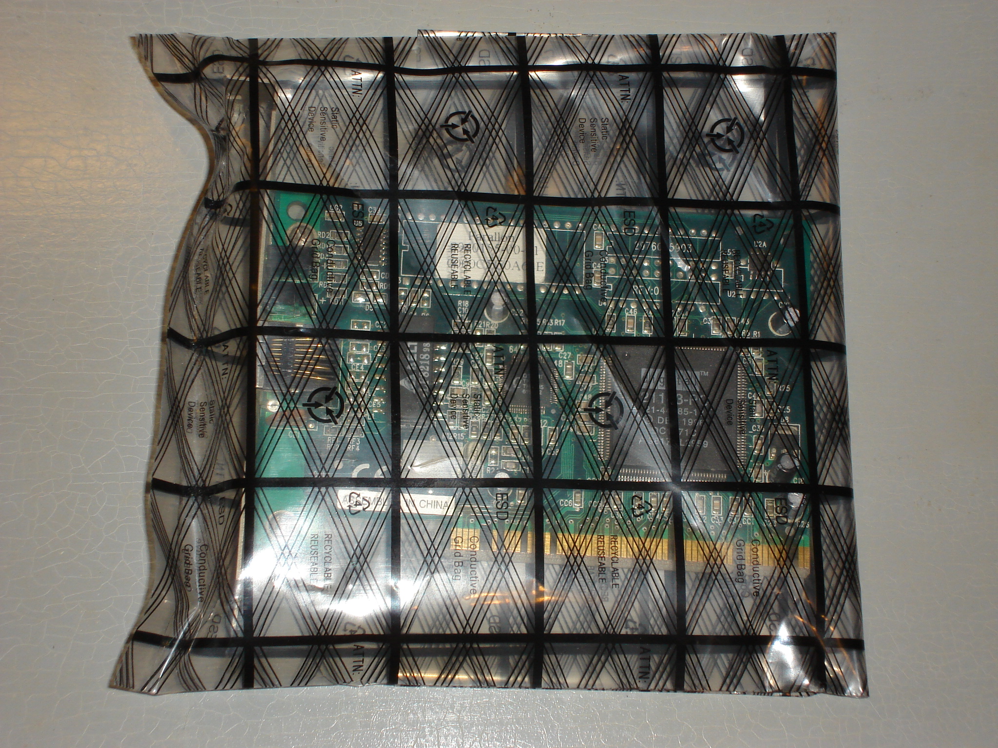
Of course, there is always the no-brainer solution which is to put the PCB inside one of these which acts as a makeshift Faraday cage. Just make sure it’s the silver ones, not pink. Also be sure it has the bubble padding to prevent the PCB from touching the conductive material.

Does anyone know the trace for the sync button?

right under the switch is a capacitor (C27), connect to the left of the capacitor (the silver side) just above the letter “C” in “C27”

Did I get it right?

No, you wanted this

Okay guys, something new for you to give a whirl. I was going to do a whole blog post on the process but got side tracked after doing this, so here’s the gist.

I decided to just delve into how the sub-board operates and check the signals for anything we could use to easily disable it, got tired of guessing. Turns out I was right, there’s an initial transaction from the main micro, and passes security information when plugged into the XB1 system. However, they appear to have kept it surprisingly simple, only uses 2 lines, and doesn’t require a separate clock signal. It’s like dedicated lines, one for input info, and one for the output.

The details on these transactions is hard to say, it’s even hard to currently say which direction these are occurring other than some educated guessing. However, one signal in particular stuck out, it’s a clock that almost looks like it comes from the main micro so that the sub-board can take in the information and zip it off to the system. This includes some handshaking initially as well as of course the input information later on. It makes sense since there’s a shitload of information and it needs a proper clock to ensure the data sync is correct. There’s way more to this back and forth, but for us, that’s all we want. The clock is 8Mhz for those curious.

That’s the Achilles’ heel. Kill the clock, and the information instantly becomes garbage.

Here is the spot you want to disconnect, cut the trace stemming from this pin and the clock is severed, rendering the data worthless and the pad unable to sync wirelessly anymore.

Alternatively, we could probably just ground the pin through a resistor also, say 500-1k in case it’s an actively driven signal, and that could probably work too. I didn’t try it, instead I just cut the trace to ensure this theory worked. Plugged in the USB, worked fine, unplugged and plugged into my PC, held the home to start the sync process, and nada. It’ll blink the home LED for a while until it times out, and that’s that.

I cut the trace on the opposite side in the picture, right after the via, this allows you to lay the PCB flat since the analog cubes makes it a little awkward to cut that particular point, not to mention the trace run to that via’s fairly short and there’s other stuff you could accidentally cut.

TL;DR: Cut the trace and the wireless is bye bye.
Great detective work, I knew a clock would be the key, but color me a bit confused. This clock is, or isn’t, required for communication between the MCU and the subboard for security authentication purposes? If not then I question if the subboard is doing any auth at all unless MS is doing clockless data communication with their security keys which requires precise propagation delays or if the authentication is nothing more than setting the right analog levels; both extremely doubtful.

Could you do me a favor and see what clock frequency the Y1 oscillator is running at; I’m real real curious if it’s in the same 8MHz range; the only equipment I have at home goes up to 100Khz. If it’s not, it’s still like likely to be the source, just down sampled by the subboard’s MCU. If so, solder bridging pins 2 & 3 of Y1 would kill it at the source and shouldn’t harm anything as it’s just a glorified tuning fork so it should be reversible. I guess I could just get off my ass and open up my stick and see what happens when I short it.

The way it works is this, and I’ll post up screenshots later when I do a full breakdown of my reasoning.

Wireless boot:
2 pin, clockless communication between the main micro and the sub-board. It’s a short spurt of data, but definitely not just states.

Wired boot:
2 pin, clockless communication between the main micro and the sub-board. Longer spurt of data which probably contains the security required for wired enumeration.

Post boot wireless:
Clock signal is engaged (you can see it go high, then do it’s thing during data transfers) and used during wireless security handshaking, and then finally user information (buttons, etc).

Post boot wired:
Nothing, states are steady, clock signal is never engaged. This is what we are trying to emulate in the other mode.

Now, what this means is that the sub-board uses the oscillator as it’s main method of clocking data, but internally to the sub-board. The main micro sends it’s spurt of data on one signal, and is then sent back data over the other signal. No third clock signal is ever used, but if you kill the oscillator the sub-board will probably not be able to effectively do it’s thing and will just cease to function in both wired and wireless modes.

I was worried I’d see something else during this whole investigation, but once I saw the clock signal was only used during wireless it was an easy jump to deduce the best way to do this.

You’re probably right, the main oscillator likely runs at 40Mhz, since the 8Mhz generated clock can be sampled easily at that speed.

I see, very interesting, I look forward to seeing the details, especially O-scope shots of the data lines if you have those.

By the way, totally disregard my statement about no discrete clock signal meaning it’s clock-less data communication or simply level-based. It’s very likely that the data has the clock encoded in the data ala Manchester encoding or even more likely an RS-232 like signaling mechanism with start and stop bits to sync the two devices without needing a clock.

The only thing that worries me slightly about cutting that trace is that there is still likely to be spectral energy at 2.4GHz. That energy will be nonsensical but it still may cause some sort of interference due to its mere presence. Killing the oscillator will eliminate this possibility, but I’ll have to make sure it doesn’t eliminate it from working altogether. I don’t have a spectrum analyzer at my disposal but if one did, hooking up to the micro SMA connector along the antenna path would give you that answer (assuming that trace wasn’t cut.) Perhaps this is so into the weeds for any tournament organizer who wouldn’t know the difference either way as long as it doesn’t connect over wifi.

In any case I’ll have some free time tomorrow to play doctor with it. I just hope I don’t make the red nose light up for the last time.

Grammaton & Phreak, reading what you guys are thinking/finding is crazy cool :slight_smile:

It’s possible that it’s still trying to send out the garbage data, but I wouldn’t worry about it. I think that the inability to even process the incoming data will stop it from moving it to the wireless protocol they have going. Without being able to move it, nothing gets sent.

Honestly though, at a tournament there’s more radiated emissions from the gazillion devices running at these frequencies anyway. FCC regulations are pretty darn strict on these kinds of devices, so I wouldn’t sweat it.

Wish I had one of these to make sure, hah.

It’s fun to work out a problem like this once in a while and really think it through, as long as you have the tools to test theories anyway.

If someone gives this a shot, post up if it works for you so that I’m not crazy about what I saw, hah.

I agree. It’s an incredibly interesting read. What will be revealed next? Haha. Better than Days of Our Lives.

Hey everyone! I’m planning on dual-modding my Madcatz 360 sticks (ssf4 te-s and sfxt pro) with XB1 PCBs in the next month or so. I want to keep it pretty simple. Just dpad, 6 buttons, Start, Select, and Guide and a 4PDT switch for the USB cables. I’ve looked over this thread pretty extensively, but I’d like some input about the following supplies:

  1. Solder - brand, thickness, type
  2. Flux - Is it necessary if using rosin core solder? If so, what is recommended?
  3. Wire - guage, solid or strand (maybe cat5?)
  4. Iron tip - Flat or round?

Additionally, I see that on the madcatz boards there are grounds labeled KGRD and GRD. Do these need to be handled independently or can I essentially daisy chain them going into the XB1 board? I don’t want to short them when in 360 mode.

Thanks guys!!!

One other question: Any input on a recommended temp for the iron?

if you’re not comfortable soldering i wouldnt recommend starting with this pad

  1. Brand does not matter. You want rosin core, 0.020" to 0.032" diameter. Lead/tin alloy works the best but is banned in many countries (RoHS rules) tin/silver alloys will work too but is harder to work with.
  2. Yes and No. Knowing when and when not to use additional flux is something you got to learn on your own unfortunately. It is more art than science, typically if you using rosin core solder you don’t need additional flux. Espesically with a project like the Xbox One pad hacking.
  3. Gauge? Typical stick mods use a 26 to 28 gauge wire, stranded as solid wire has a tendency to break. For the Xbox one pad hack you want to go with a 28 to 32 gauge (30 and up is a pain in the ass to work with)
  4. Iron tip, you want to use the smallest tip you can that provides the most even heating. Wider tips heat more surface area, but you do not want your tip any bigger than the spot you are trying to solder too.

kgnd is for the Start, Select and Home buttons, the tournament lock out open the circuit and disables the start and select use. You can bridge the gnd and kgnd but you lose the tournament lock

I would Follow Vicko’s advice, the Xbox one Pad hack is not a project for starting out.
Skill wise this is a very advanced hack, and some of the more experienced moders are even having some issues.

I actually had a much easier time when I started using flux with the rosin core solder. Also, things went a lot smoother when I switched to 30gauge solid core (although I’d imagine 28 would’ve been better).
To each their own I guess :slight_smile: