On this pcb layout
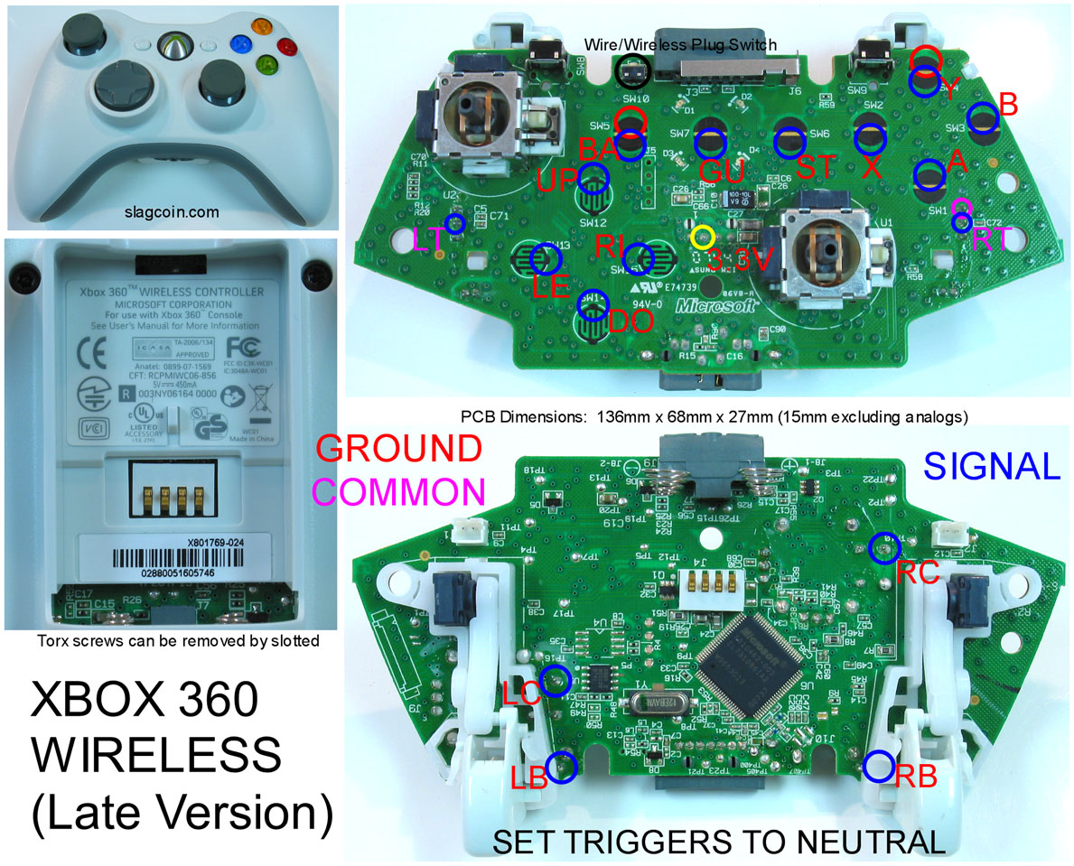
There is a spot on the back for the LB and RB signal points and then there is LC and RC. What is that, alternate bumber signal points ?
On this pcb layout
There is a spot on the back for the LB and RB signal points and then there is LC and RC. What is that, alternate bumber signal points ?
I thought it was Right Click and Left click, via when you push the analogs down
indeed it is my friends
Good look thanks.