Great job on getting this torn down and finding all the connection points for all to see. This is definitely a more demanding job than the XB1’s PCB, it’s very much akin to being forced to solder to the mezzanine connectors in which case I would definitely recommend people use some solid 30AWG wire.
I’m fairly certain the reason is a bit more complicated than that. With no DS4 on hand I took a look this teardown video and if you pause it at 11min 37sec (where I linked it) you can get a pretty decent view of the conductive button sheet, specifically all the left-side buttons including L1 & L2. I colorized all the relevant traces as can be seen in the pic beow.
What you’ll notice is that the L1 (and presumably R1) buttons look markedly different from the other buttons. Where the standard buttons are cut into semi-circles, the L1 button looks like a maze. The standard semi-circle buttons are digital (i.e on or off) and share a common return line (colored green). However, this L1 button is analog; i.e. it could be a range of values. This is very much akin to the XB1 pad where the triggers are analog via the hall sensor and the other buttons are digital. The maze pattern actually makes the button into a variable resistor and thus pressure sensitive; the harder your push the button the less resistance the button has.
So what you have is Vcc connected to one side of a variable resistor (L1 button) and then the other side of the variable resistor is connected to a fixed-value resistor (colored purple) which then leads to L2’s return line. That is nothing more than a voltage divider! If you read my posts on the XB1 pad hack thread, you’ll notice that voltage dividers come up quite often in circuits like these.
So here is what I believe is going on:
[list]
[]The red trace is powered up to Vcc
[]The signal for L1 is the yellow trace
[]With no pressure on L1, the maze is at a very large resistance and effectively acts as an open circuit between Vcc and the signal side (yellow trace).
[]With no path between Vcc and the yellow L1 signal trace, the voltage of this trace is pulled down to L2’s return line (blue trace) through a fixed resistor (purple). Thus no button press == 0v
[*]When pressure is put on the maze it’s resistance starts to drop quite rapidly and thus the voltage of the line will start to increase as you change the ratio of the voltage divider. Thus button press == some positive voltage no greater than Vcc.
[/list]
I’m curious, what were the model numbers of the two that didn’t work and what was the model of the one that did work? Inverter IC’s come in a few different flavors: Totem-pole output, Open Collector Output and Schmidtt Trigger Output to name a few off the top of my head. Knowing which one worked and which one didn’t would be useful in knowing what the DS4 is doing on the MCU side of things.
Super interesting post, G.Klerik (btw, I love “Equilibrium” too. A pity the film is not more famous). However, given what you explained, inverting the inputs for L1/R1 should have worked, shouldn’t it ? I could imagine a problem with “low speed inverters” but not in this context.
L1 and R1 are not analog. It was already announced that the DS4 will be using digital buttons instead of analog buttons like the DS3. The only thing still analog is L2 and R2.
Plus if you look at the rubber membrane sheets you would notice all the rubber contacts are flat (including L1/R1) except L2/R2 which are domes . The roundness of the dome is what is causing the change in contact surface area as more pressure is applied.
Ok, so what button is the one with the maze-like pad that I’ve been referring to? Is that L2/R2? I’ve never owned a PS so everything I’m going off of is literally from that video
Reminds me of the DS3 traces. I got 99% done and then the last one was pulled out by the wire. Then broke off. What a huge pain in the ass. I bought Sixaxis after that and left the ribbon connector on, cut off the plastic from the top of it, and soldered direct to the contacts.
That button is L1. Just because it has a maze-like pad doesn’t mean its an analog button. 360 Fight pads do maze-like contacts for its face buttons. 360 wireless MS pads with the transforming dpad has maze-like contacts for its dpad. There are countless other controllers that use maze-like contacts for their buttons and are digital. I’m pretty sure having a maze-like pad would mean that it isn’t an analog button.
The L2/R2 buttons on the DS4 have a resistor (7k ohm IIRC) that connects the two sides of the button contacts. The trigger pads look exactly like all the analog pads on the DS3. I’m pretty sure when you are pressing on the triggers it lowers the resistance. The harder you press the lower the resistance goes.
Any word yet on how optical joystick PCB’s such as the SPARK work with the DS4? I would like to do a DS4/PS360+ dual mod and be able to keep using my SPARK PCB’s
Thanks for the follow-up, consider me corrected. So just for my own curiosity, what is that element that I highlighted in purple and called a resistor? It seems that you are saying that the true resistor is the horizontal rectangle between the blue and light blue trace at the top?
For this application an N-channel MOSFET would be the best type of transistor in my opinion. If you choose the right one carefully you’ll only need a single resistor to make an inverter. Something like the SUP50N03-5M1P aught to do the trick. Here is the simple schematic and SPICE simulation. I’m assuming that the L1/R1 buttons go to 3.3V and that you tie VDD to the USB’s 5V.
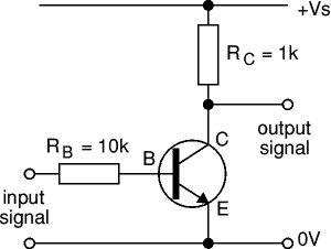
Ive been using general purpose NPN transistors, but with a 10k ohm resistor on input. I also prob should be using 1k ohm on the vcc line, but am using 10k there as well due to what I have in stock.
So input is wired to the button and output is wired to the button contact on the ds4.
So given the info you provided plus the screen shot of the trace that I posted, here is the circuit for L1 & R1 as I see it. Since L2 is a variable resistor that decreases with pressure, I ran the simulation 9 times - each time reducing the resistance of L2 by 500 ohms starting at it’s resting value of 8.5k. I also simulated an L1 pad press at 12ms. You’ll notice that Pin2 does indeed go from 0v to 5v when pressed (active high). Also as the resistance of L1 goes down, as when being pressed, the voltage also goes down towards 0v (active low.) One thing to note is that there actually are 9 traces for Pin2 but they are all stacked up on each other since they are the same value so it looks like a single trace.
In order to get this to work I assume three things:
[list]
[]Pin 1 is pad ground
[]Pin3 must be where Vcc is supplied. I choose 5v for my simulation but it may very well something else like 3.3v. Can you confirm actual voltage when powered?
[*]Pin2 must have some resistor pulling it to ground because when the L1 button is not being pressed, Pin2 would be floating otherwise. If Pin2 leads directly to the MCU then it will be the input resistance of MCU input pin that pulls it down. I choose a value of 1k for the sim, but the input resistance of the MCU would be much,much higher on the order of 100k to 1MEG. Either way, its value really doesn’t matter all that much for simulation purposes.
[/list]
Finally, you can confirm that my circuit is correct if you measure Pin4 to be very close to Vcc/2 when no buttons are pressed. That is it should be half the voltage of whatever Pin3 is. This is because Pin4 is the output of a voltage divider where both resistors are almost equal in value at rest (8.52k & 8.3k). Both resistors are likely to be 8.5k with 2% tolerance.
This DS4 pcb… this isn’t tech, this is art. Sony you guys have some MAGNIFICENT engineers working for you. Mona Lisa? More like shit dead art, they should hang a screen cap of gummo’s post so everyone can understand just how amazing the PCB is
The DS4 PSB might look cooler from an aesthetics point of view (to some) but the XB1 pad is much, much more elegant from an engineering standpoint. There are no ribbon cables, no conductive pad layer just two PCB’s that join at the hip via two mezzanine connectors. Even the wifi components were put on its own floating island surrounded by a thick ground shield trace to minimize interference. It’s very apparent that MS put in over a million to design this new pad. They will recoup that cost in no time with how much cheaper it must be to manufacture.
Take a wire from Vcc to a 1K resistor to the collector of the transistor
take a wire from the emitter to ground?
take a wire from the base of the transistor to a 10k resistor to another wire going to the button?
Do you just splice the Vcc wire found in the micro USB section, or are there any other Vcc points that we could use for the L1/R1 buttons? I’m asking because that’s 3 Vcc points we need (2 for both buttons, and one for the pcb)
Yes on #1 - #4, no idea on #5 as I don’t have a DS4 so gummo will have to field that one.
Note that the comments on that NPN reflect that these things are very sensitive to heat and more than a few people have killed them when trying to solder. If you have a Fry’s nearby, I would recommend getting your parts there as they carry NTE which although not great is generally of higher quality than radio shack stuff. If you plan to order online then I would suggest you order that NMOS I posted from digikey which will get you the same net result with one less resistor.
I tap whatever Vcc spot is the most convenient and wire it to the inverter circuit. Then wire both resistors together. Ill be posting a picture of my setup for the circuit. I do like a dead bug approach.