I wrote this in laymen terms as much as I could so more people can grasp what being said. I know it is not 100% accurate, I left some stuff out and fudge some details.
In actuality what is being sent back and forth is binary code, but often programmers look at the packets being sent back and forth in hexadecimal notation.
Here is a sample of PS2 Protocols http://store.curiousinventor.com/guides/PS2/#low_level
I don’t think so. Everything the microcontroller is doing is way too fast to become noticeable lag. Clock rate should be on the order of MHz, communication at 100s of kHz, and even if it’s doing ADC that should be at least kHz. There’s tons of time to do everything it needs and still beat the 1/60 s framerate by a couple orders of magnitude.
I know the Left analog on a toodles board as no lag, as in synch with the POV Hat.
You think just because of the high clock cycles their shouldn’t be lag, but I can’t ignore the complaints of people either.
With the clock cycle argument we should have Zero lag in any converter or stick or pad.
I am not even sure which side holds more weight as I have no hard evidence either way.
I can offer an explanation on how Analog works, and by extension I can explain the theory why LS would lag, I can’t prove with my resources.
I don’t argue that LS lags, I just think there’s no good reason for it :oP
I agree with that statement, Hell I make a toast to that statement.
Hey Darksakul! Thanks for putting this thread together. It’s so useful. You are awesome!
Work in Progress
Common Tools every modder needs
Guide by Lady Adafruit
Here is a similar Video by Ben heck
Copied from Dual Modding PS3 TE To Work With PS4?
That describes pad hacks right there.
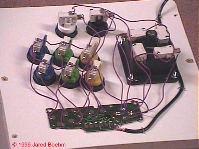
You disassemble a controller completely, get rid of the shell, the buttons and everything that isn’t electronics.
Then you are replacing those button contacts and switches for a different kind of switch. That is all a arcade button really is, its a type of switch.
Given its a momentary push switch, the moment you let go of a button the switch goes back to being OFF. It is the same thing with the rubber contacts inside of a game pad.
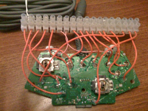
Here is a old school example of a Pad hack. This is a SNES controller stripped down to it’s printed circuit board and system cable.
Then wires are soldered to the PCB’s contacts and lead over to a set of arcade buttons.
NES and SNES controllers are as simple as it get, you could clone one with some electronic knowledge and some off the shelf shift registers.
Only controllers that are easier to hack are Atari 2600 joysticks and Neo Geo Controllers (as they usually lack a PCB)
With the PS3 and Xbox 360 Pad hacking got a bit more complex.
You had to deal with not just the digital push buttons, but analog triggers and buttons as well.
The methodology is the same, you are just mimicking a full press on the Analog buttons.

PS4 (and XBox 1) game pad PCBs are a bit complicated with smaller points to solder to.
The basics are still there but the actual skill and difficulty goes up dramatically from the Xbox 360 pad hack I showed you before.
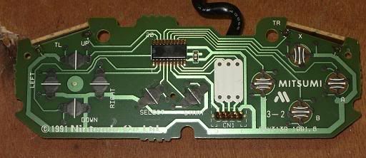
Here is a offical Nintendo SNES game pad PCB to show for comparison.
There more to Pad hacking than what I showed here, things that should be factored like common ground, analog thumb sticks and such.
It is possible to Pad hack a PS4 game pad, but its far from a beginner project. If you never really soldered before I advise you not to attempt it on your own.
You could hire someone else, buy the new Hori Hrap V4 (or the new PS3/PS4 TE 2 when it comes out) or you can wait it out for more options later.
PCB (Printed Circuit Board) anatomy

Board Material - usually made from some solid, non-conductive, material, typically glass-reinforced epoxy (FR-4)
Traces - Usually made from copper but I seen aluminium and even gold used.
Sometimes Traces are made thicker to reduce interference.
Pads - exposed metal areas of the board often plated in another metal (like tin) to provide a point for components to be soldered too.
Copper fill (also known as a Ground Plane or power Plane) - part of the same layer as the traces, these are larger sections of the PCB. The plane is often used for ground, power, thermal heat sinking or your EE teacher told you its done that way.
Vias - Vias are used in layer boards to connect one layer to another electrically. A hole is drilled in the PCB and then electroplated or a metal insert is added.
[list]
[] Through hole – Most common type of via, a hole is drilled through the whole board and then electroplated so that it is conductive.
[] Blind – A blind via is used in designs with more than two layers to connect a surface layer to an internal layer without going all the way through.
[*] Buried – Buried vias are similar to blind vias but are only used to connect internal layers.
[/list]
Soldermask - a layer on the board that applied after manufacturing. Typically green but it can be any color really.
This is to keep solder from spreading where it shouldn’t
Silkscreen (as in the printing process of the same name) - On Top of the Solder Mask, the board gets printed with markings for reference or documentation
Like you see on the SNES PCB on the post before this one.
Carbon Conductors - That black stuff on button contacts. This is to allow for electrical contacts with a rubber dome switch and the surface to be electrically conductive but not allow solder to get to that area.